Product Details
The AD664 is four complete 12-bit, voltage-output DACs on one monolithic IC chip. Each DAC has a double-buffered input latch structure and a data readback function. All DAC read and write operations occur through a single microprocessor-compatible I/O port.
The I/O port accommodates 4-, 8- or 12-bit parallel words allowing simple interfacing with a wide variety of microprocessors. A reset to zero control pin is provided to allow a user to simulta-neously reset all DAC outputs to zero, regardless of the contents of the input latch. Any one or all of the DACs may be placed in a transparent mode allowing immediate response by the outputs to the input data.>/p>
The analog portion of the AD664 consists of four DAC cells, four output amplifiers, a control amplifier and switches. Each DAC cell is an inverting R-2R type. The output current from each DAC is switched to the on-board application resistors and output amplifier. The output range of each DAC cell is programmed through the digital I/O port and may be set to unipolar or bipolar range, with a gain of one or two times the reference voltage. All DACs are operated from a single external reference.
The functional completeness of the AD664 results from the combination of Analog Devices" BiMOS II process, laser-trimmed thin-film resistors and double-level metal interconnects.
### Features and Benefits
.
Four Complete Voltage Output DACs
.
Date Register Readbck Feature
.
"Reset to Zero" Override
.
Multiplying Operation
.
Double-Buffered Latched
.
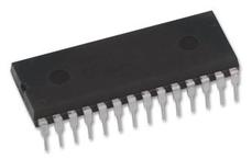
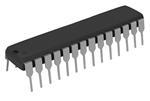
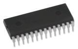
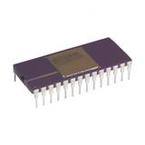
Surface Mount and DIP Packages
.
MIL-STD-883 Compliant Versions Available
查看全部
AD664JNZ-UNI 产品概述
Product Details
The AD664 is four complete 12-bit, voltage-output DACs on one monolithic IC chip. Each DAC has a double-buffered input latch structure and a data readback function. All DAC read and write operations occur through a single microprocessor-compatible I/O port.
The I/O port accommodates 4-, 8- or 12-bit parallel words allowing simple interfacing with a wide variety of microprocessors. A reset to zero control pin is provided to allow a user to simulta-neously reset all DAC outputs to zero, regardless of the contents of the input latch. Any one or all of the DACs may be placed in a transparent mode allowing immediate response by the outputs to the input data.>/p>
The analog portion of the AD664 consists of four DAC cells, four output amplifiers, a control amplifier and switches. Each DAC cell is an inverting R-2R type. The output current from each DAC is switched to the on-board application resistors and output amplifier. The output range of each DAC cell is programmed through the digital I/O port and may be set to unipolar or bipolar range, with a gain of one or two times the reference voltage. All DACs are operated from a single external reference.
The functional completeness of the AD664 results from the combination of Analog Devices" BiMOS II process, laser-trimmed thin-film resistors and double-level metal interconnects.
### Features and Benefits